Latest News

“AI is making outputs more accessible, forgetting the value of the process”
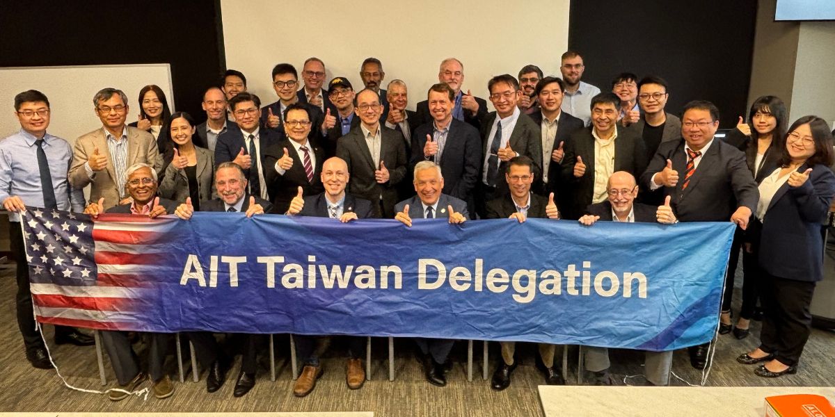
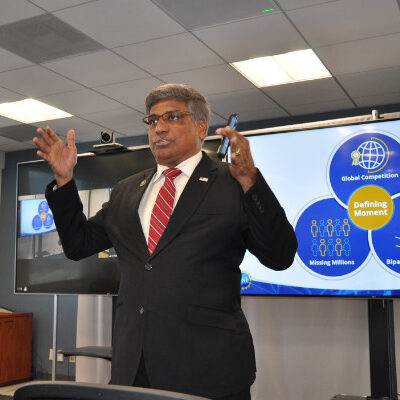
CA DREAMS welcomes AIT Taiwan Delegation

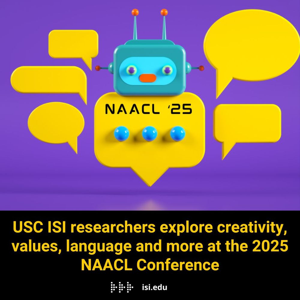
ISI at the NAACL ‘25 Conference

ISI @ the 2025 ACM Web Conference
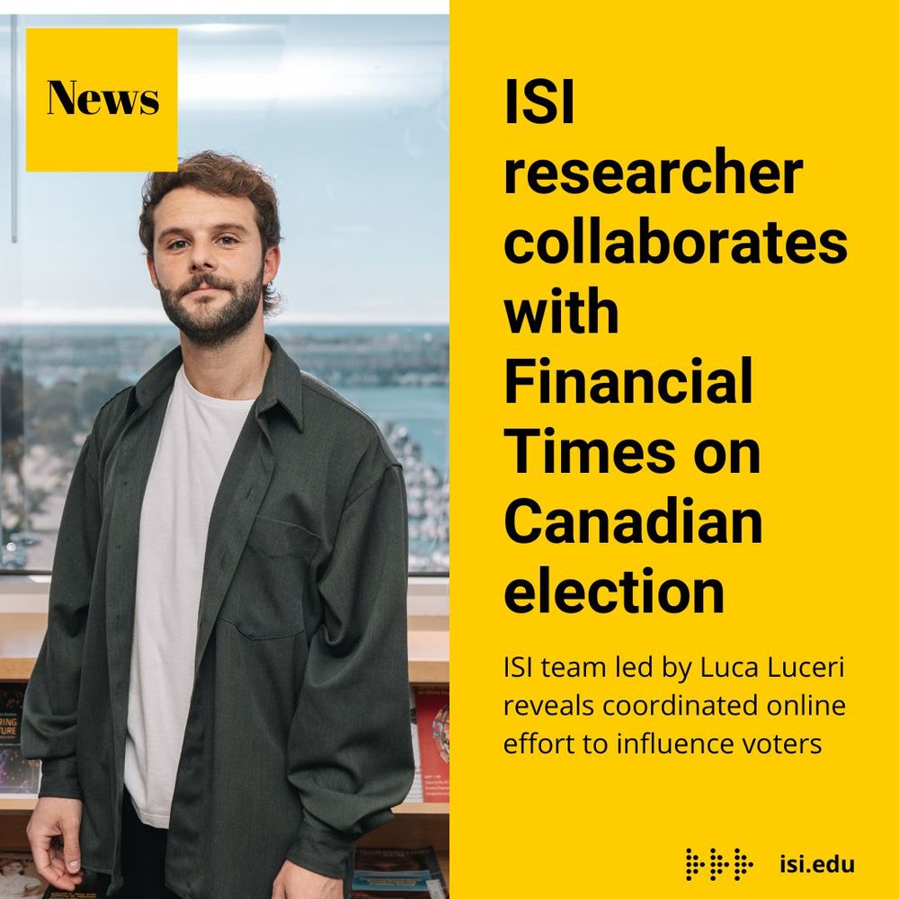
ISI researcher collaborates with Financial Times to uncover coordinated online effort to sway Canadian election
USC at ICLR 2025
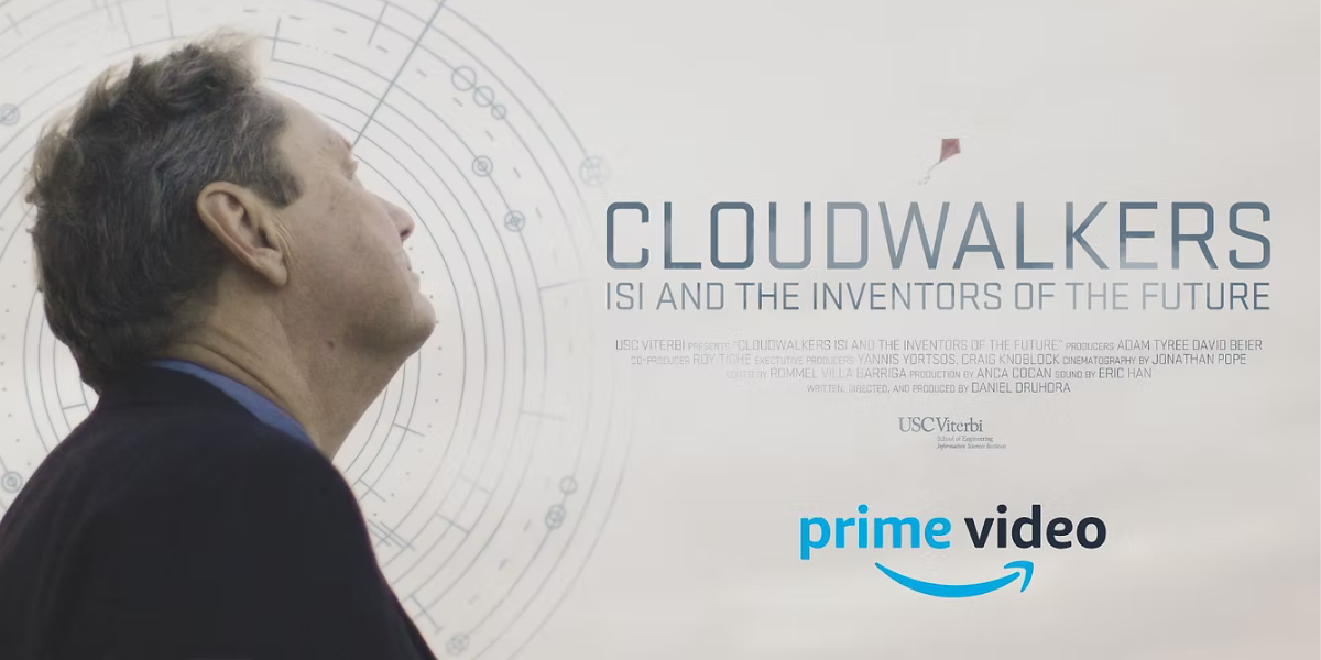
Cloudwalkers now available on Prime Video

Mapping Our Emotionally-Divided Society

Precision Chip-scale Laser Frequency Microcombs at the Fundamental Limits
Professor Chee Wei Wong, UCLA
https://usc.zoom.us/j/97017422125?pwd=Dbrt8MNMrmBV3xalKQJcAiNsggFJjJ.1&from=addon
-

Antimonide-based Narrow Bandgap Semiconductors for Infrared Technology and Quantum Information Science
Dr. Minh Nguyen, HRL Laboratories
https://usc.zoom.us/j/97017422125?pwd=Dbrt8MNMrmBV3xalKQJcAiNsggFJjJ.1&from=addon
-
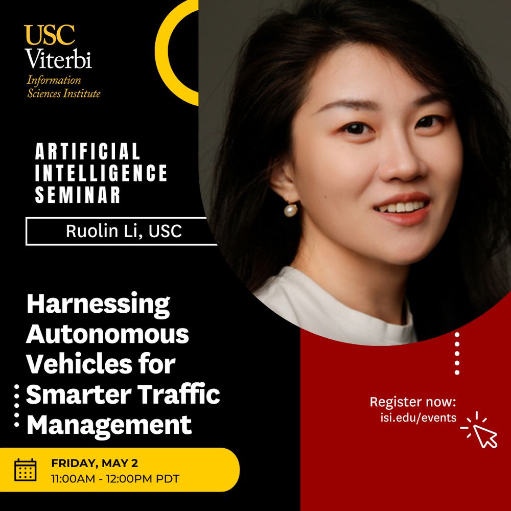
Ruolin Li is a Gabilan Assistant Professor at USC. In this seminar, she'll examine a series of representative transportation scenarios to explore how AVs can be leveraged to improve traffic efficiency and overall system performance.
Join here: bit.ly/3GzD2Oi
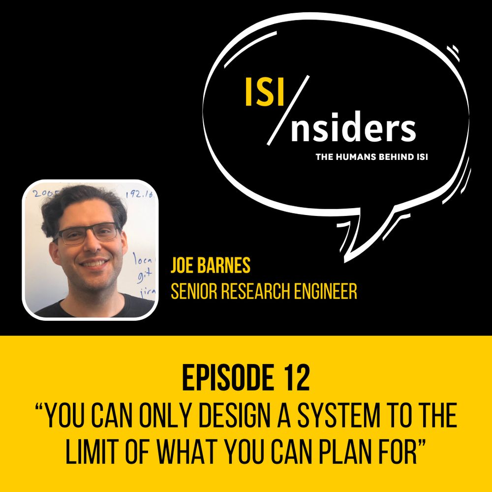
In this episode, Joe Barnes, a Senior Research Engineer at ISI, describes how thinking of concepts in terms of systems has extended to parts of his life outside of work.
Listen here: bit.ly/4k0fq3H
🔗 Read more: bit.ly/4jGOvKv
@viterbischool.usc.edu
@usc.edu
@csatusc.bsky.social
#NLP #AI
Read about it here: bit.ly/3Sb598U
@luceriluc.bsky.social @usc.edu @viterbischool.usc.edu
Check out the research spotlights: bit.ly/435bQzE

Delivering the future
ISI's mission is to advance society through pioneering research and technological innovation. We cultivate an intellectually vibrant environment where researchers are empowered to imagine bold solutions to complex problems and to develop into world-class leaders. Guided by integrity, inclusion, and a commitment to excellence, we create unprecedented capabilities that harness information to transform lives.
Research & Development
Part of the University of Southern California’s Viterbi School of Engineering, ISI is a pioneer in research and development across an exceptionally wide range of advanced information processing, computer, and communications technologies.
Our broad expertise spans artificial intelligence, computational systems and technology, space engineering, informatics systems research, and networking and cybersecurity. Bridging multiple technology disciplines through both academic and industry expertise, ISI continues to shape the technologies of tomorrow.

Centers
ISI Centers are internationally renowned for pioneering research in a multitude of areas and disciplines, with collaborations with Lockheed Martin, Raytheon, Northrop Grumman, and numerous other organizations. From quantum computing to global space applications, ISI Centers push forward the boundaries of innovation.
MOSIS
In 1981, a request from DARPA led to USC establishing The MOSIS Service at ISI — a silicon prototyping and low volume production service for custom and semicustom integrated circuits.
Over the past 40 years, The MOSIS Service has collaborated with over 50 US government laboratories and agencies, 800 domestic and foreign colleges and Universities, and more than 100 commercial companies, and continues to support the advancement of microelectronics.


Join the Future
To build upon its successes and global reach, ISI actively recruits exceptional talent. We are dedicated to investing in tomorrow’s leaders, providing numerous internship, job, and program opportunities for students, as well as unique opportunities for exceptional researchers in information sciences and related fields.
Featured Job Openings
To build upon its successes and global reach, ISI actively recruits exceptional talent. We are dedicated to investing in tomorrow’s leaders, providing numerous internship, job, and program opportunities for students, as well as unique opportunities for exceptional researchers in information sciences and related fields.
ASIC/FPGA Research Engineer - Digital Design
Arlington, VA
Hybrid Eligible
Perform front-end digital design of advanced ASIC or FPGA-based prototypes addressing problems of national importance while developing novel computer architectures, RTL models, and systems-on-chip.
Transformational Computer Engineer
Arlington, VA
Hybrid Eligible
Information processing capabilities are more important than ever, including hardware architectures and systems-on-chip that can reach new heights of efficiency, security and more. Such problems of national importance are being tackled by ISI.
Computer Scientist - EDA Researcher
Arlington, VA
Hybrid Eligible
The Reconfigurable Computing Group (RCG) at ISI is a leader in disrupting and advancing the fields of front-end ASIC and FPGA design, reconfigurable architectures, and EDA tools. We are currently recruiting for an EDA Researcher to join the team.
Did you know
ISI SEMINAR SERIES
Keep up-to-date with the ISI seminar series by subscribing below.
You will have the option of subscribing to individual seminar topics.
subscribe to notificationsISI SEMINAR SERIES
Keep up-to-date with the ISI seminar series by subscribing below.
You will have the option of subscribing to individual seminar topics.
Information Sciences Institute
As a world-class institution, ISI offers a prestigious, intellectually vibrant environment, combining the best of major research universities and industry labs on both coasts.
ISI is committed to forging a better future. Please visit our careers web page to learn how you can become a part of the ISI community.